An integrated circuit (IC) is a complete electronic circuit built on one small piece of semiconductor, usually silicon. It packs transistors, resistors, capacitors and the wiring between them into a single chip. That chip can amplify a signal, store data, keep time or run a full computer program.
What an integrated circuit actually is
Before ICs, engineers built circuits from separate parts. Each transistor, resistor and capacitor was its own component with its own leads, soldered to a board. A radio might need dozens of them. An early computer needed thousands, and every solder joint was a possible failure.
An integrated circuit puts all of those components on one slab of silicon at the same time, during manufacturing. Nothing gets soldered together inside. The parts are formed in the material itself, and microscopic metal tracks connect them.
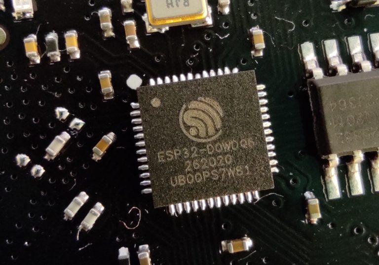
People use a few terms for the same thing. “IC,” “integrated chip,” “microchip” and “chip” all mean an integrated circuit. Strictly, the chip is the bare silicon, called the die. The black plastic body with legs is the package that protects the die and connects it to the outside world.
The basic structure of an IC
If we could slice through a typical integrated circuit, we would find three main zones.
The silicon die. This is a thin, flat square of very pure silicon, often only a few millimetres across. Its surface has regions “doped” with tiny amounts of elements such as boron or phosphorus. Doping changes how easily silicon conducts electricity, and that is what makes transistors and diodes possible.
The interconnect layers. Stacked on top of the transistors are layers of metal wiring, usually copper in modern chips, separated by insulating layers. A modern processor can have more than ten of these metal layers. They route signals between billions of transistors, much like a multi-layer circuit board shrunk thousands of times.
The package. Fine bond wires, or tiny solder bumps, link pads on the die to the pins or balls of the package. The package carries heat away, blocks moisture and gives us something we can actually handle and solder.
How IC chips work
Nearly everything an integrated circuit does comes down to transistors. In digital chips, a transistor acts as an electrically controlled switch. Apply a voltage to its gate and current flows between the other two terminals. Remove it and the current stops.
One switch is not very useful. Combine a few and you get logic gates. Combine gates and you get adders, counters and memory cells. Combine millions of those and you get a processor.
Worked example: a NAND gate from four transistors
Most digital ICs use CMOS (complementary metal-oxide-semiconductor) technology. CMOS pairs two transistor types: N-channel, which turns on when its gate is high, and P-channel, which turns on when its gate is low.
A two-input NAND gate uses four transistors:
- Two P-channel transistors sit in parallel between the supply voltage and the output.
- Two N-channel transistors sit in series between the output and ground.
Now walk through the inputs. If both inputs are high, both N-channel transistors turn on and pull the output to ground, so the output is low. If either input is low, at least one P-channel transistor turns on and pulls the output high. That is the NAND truth table: output low only when both inputs are high.
The familiar 74HC00 chip holds four of these gates in a 14-pin package. That works out to 16 transistors for the logic, plus a few more for input protection. NAND is “universal,” so every other logic function can be built from it. Scale the same idea up and you reach the arithmetic units inside a microcontroller.
Analog ICs work differently
Not every integrated circuit switches between high and low. Analog ICs use transistors in their in-between region, where a small change at the input causes a proportional, larger change at the output. An op-amp such as the LM358 uses this to amplify sensor signals. Voltage regulators use it to hold an output steady while the input wanders.
A short history: from one transistor to billions
Jack Kilby at Texas Instruments demonstrated the first working integrated circuit on 12 September 1958. It was a small oscillator built on germanium, with parts connected by hand-attached gold wires. Kilby later received the 2000 Nobel Prize in Physics for the invention.
Months later, Robert Noyce at Fairchild Semiconductor designed a silicon IC whose connections were deposited as a flat metal layer. His design used the planar process developed by his colleague Jean Hoerni. That flat, printable approach is the ancestor of every chip made today.
In 1965, Gordon Moore observed that the number of components on a chip was doubling every year. He revised it to every two years in 1975. “Moore’s Law” was never a law of physics, but the industry treated it as a target for decades.
The numbers show how far it went. Intel’s 4004 microprocessor, released in 1971, had about 2,300 transistors. Today’s largest processors carry more than 100 billion.
Levels of integration
Engineers used to group integrated circuits by how many gates or transistors they held. The exact boundaries vary between textbooks, but the classic scale looks like this:
| Level | Rough size | Typical example |
|---|---|---|
| SSI (small-scale) | Up to about 10 gates | 74HC00 quad NAND |
| MSI (medium-scale) | About 10 to 100 gates | Counters, multiplexers |
| LSI (large-scale) | About 100 to 10,000 gates | Early microprocessors like the 4004 |
| VLSI (very large-scale) | Over 10,000 gates | Modern CPUs, microcontrollers, GPUs |
Almost everything designed now counts as VLSI, so these labels matter mostly for reading older datasheets and textbooks.
How integrated circuits are made
IC manufacturing happens in fabs, factories where the air is far cleaner than in an operating theatre. A single speck of dust can ruin a chip. The process, simplified:
From sand to chip
- Refine silicon to extreme purity and grow it into a single-crystal ingot.
- Slice the ingot into thin wafers, commonly 300 mm across.
- Grow or deposit a thin insulating layer on the wafer.
- Coat with light-sensitive photoresist and expose it through a patterned mask.
- Etch away the exposed areas to transfer the pattern into the wafer.
- Dope selected regions by firing ions into the silicon.
- Repeat patterning, etching and deposition for every layer, including the metal wiring.
- Test each chip on the wafer, cut the wafer into dies, then package and test again.
Step 4, photolithography, sets how small features can be. The most advanced fabs use extreme ultraviolet (EUV) light with a wavelength of 13.5 nm. One wafer can hold hundreds of dies, which is a big reason ICs are so cheap per transistor.
A quick note on “nanometre nodes.” Names such as 5 nm or 3 nm are now marketing labels for a generation of process technology. They no longer match any single physical dimension on the chip.
Classification of integrated circuits
There are several useful ways to sort integrated circuits.
By signal type
– Digital ICs work with two voltage levels representing 1 and 0. Examples: logic gates, memory, microcontrollers.
– Analog ICs handle continuous voltages. Examples: op-amps, voltage regulators, audio amplifiers.
– Mixed-signal ICs combine both. Analog-to-digital converters and most microcontrollers fall here, since they read analog sensors and process the results digitally.
By function
Microcontrollers, microprocessors, memory, power management, interface chips, sensors, timers and display drivers. A 16×2 character liquid crystal display (LCD), for example, carries its own controller IC so our microcontroller only has to send simple commands.
By package
| Package | What it looks like | Hand-solderable? |
|---|---|---|
| DIP (dual in-line) | Two rows of legs, 2.54 mm apart | Yes, fits breadboards |
| SOIC | Smaller gull-wing legs at the sides | Yes, with a fine tip |
| QFN | Flat pads underneath, no legs | Hard, needs hot air or reflow |
| BGA | Grid of solder balls underneath | Not practical by hand |
DIP chips are the friendliest for beginners. A decent soldering iron with a fine tip handles SOIC too, once you have some practice.
Integrated circuits on a maker’s bench
Most of the chips we use in Arduino projects and Raspberry Pi projects fall into a handful of families. Here are five worth knowing:
| Chip | Type | What it does | Supply |
|---|---|---|---|
| ATmega328P | 8-bit microcontroller | The brain of the Arduino Uno, 32 KB flash, 2 KB RAM | 1.8 to 5.5 V |
| RP2040 | 32-bit microcontroller | Dual Cortex-M0+ at 133 MHz, used on the Raspberry Pi Pico | 3.3 V I/O |
| NE555 | Timer | Pulses, delays, oscillators | 4.5 to 16 V |
| 74HC595 | Shift register | Turns 3 pins into 8 outputs | 2 to 6 V |
| LM358 | Dual op-amp | Amplifies and compares analog signals | 3 to 32 V single supply |
The 555 timer is a good reminder of how long a well-designed IC can last. Hans Camenzind designed it for Signetics around 1971, and it still sells in huge numbers.
A microcontroller’s general purpose input output pins are the IC’s direct link to the outside world. Each pin connects through protection diodes and driver transistors on the die. That is why they have strict current limits.
Power check
The ATmega328P allows 40 mA absolute maximum per I/O pin and 200 mA total through its supply pins. RP2040 pins are 3.3 V only and are not 5 V tolerant.
How to read an IC and its datasheet
Our own angle on this topic: knowing how a chip works matters less on the bench than knowing how to read one.
Find pin 1. Look for a dot, a dimple or a notch at one end of the package. On a DIP chip with the notch facing up, pin 1 is top left. Pins count down that side, then continue up the other side, anticlockwise when viewed from above.
Decode the part number. Take “SN74HC595N.” “SN” is the maker’s prefix (Texas Instruments here). “74” is the logic family series. “HC” means high-speed CMOS. “595” is the function. The trailing “N” indicates the DIP package. Other manufacturers use different prefixes and suffixes, so check the datasheet.
Read three sections first. Pin descriptions, absolute maximum ratings and the recommended operating conditions. Absolute maximums are limits that damage the chip. They are not targets to design to.
Maker tip
Put a 100 nF ceramic capacitor between each IC’s supply pin and ground, as close to the chip as possible. It soaks up fast current spikes and fixes a surprising number of random resets and glitches.
Advantages of integrated circuits
- Size. A chip a few millimetres across replaces boards full of separate parts.
- Cost. Making hundreds of dies per wafer drops the cost per transistor to almost nothing.
- Reliability. Fewer solder joints and connectors means fewer points of failure.
- Speed. Short internal connections let signals travel faster and switch at higher frequencies.
- Power efficiency. CMOS logic draws very little current when it isn’t switching.
- Matched parts. Components formed side by side on one die behave alike, which analog designers rely on.
Disadvantages of integrated circuits
- Limited power handling. Small dies struggle to carry heavy current or shed large amounts of heat. Big motors and loads still need separate power transistors or driver stages.
- Hard to make large inductors and capacitors. These usually stay off-chip.
- No repairs. If one transistor inside fails, the whole chip is scrap.
- Fragile inputs. Static discharge from our fingers can damage CMOS chips long before we feel a spark.
- Huge upfront cost. Designing a new chip and building masks costs millions, so custom ICs only make sense at volume.
Common mistakes beginners make with ICs
- Inserting the chip backwards. Reversed power usually kills it within seconds, and it often gets hot enough to burn a fingertip.
- Leaving CMOS inputs floating. An unconnected input drifts and causes erratic behaviour. Tie unused inputs to ground or the supply.
- Driving loads straight from logic pins. A 74HC595 is limited to about 70 mA through its supply pins in total. Use transistors or a driver chip for LEDs at higher current, relays and motors.
- Mixing 5 V and 3.3 V logic. A 5 V signal into a 3.3 V chip like the RP2040 can destroy the pin. Use a level shifter or a voltage divider.
- Skipping decoupling. No capacitor, mystery bugs.
The future of integrated circuits
Shrinking transistors is getting harder and more expensive, so the industry is pushing in other directions.
New transistor shapes. Samsung began production of gate-all-around transistors at its 3 nm node in 2022, and TSMC and Intel are moving the same way. Surrounding the channel on all sides gives better control and less leakage than the older FinFET design.
Chiplets. Rather than one giant die, designers combine several smaller dies in one package. AMD’s Ryzen processors have used this approach since 2019. Smaller dies mean better yields and the freedom to mix process technologies.
3D stacking. Memory makers already stack dies vertically. Logic is following, with layers bonded directly on top of each other to shorten connections.
Specialised chips. Graphics processors, AI accelerators and dedicated video encoders do specific jobs far more efficiently than general-purpose CPUs. That trend reaches makers too, with microcontrollers now shipping with built-in Wi-Fi, Bluetooth and machine-learning instructions.
FAQ
What does IC stand for?
IC stands for integrated circuit. The terms integrated chip, microchip and chip refer to the same kind of part.
What is an integrated circuit made of?
Mostly silicon, doped with small amounts of other elements to form transistors and diodes. Copper or aluminium layers provide the wiring, and silicon dioxide or similar materials insulate the layers. The die then sits in a plastic or ceramic package.
Is a microcontroller an integrated circuit?
Yes. A microcontroller such as the ATmega328P or ESP32 is a single integrated circuit containing a processor, memory, timers and input/output hardware on one die.
How many transistors are in an integrated circuit?
It ranges enormously. A simple logic chip has a few dozen. Intel’s 4004 had about 2,300. The largest modern processors hold more than 100 billion.
Can integrated circuits be repaired?
No. The components are formed inside the silicon, so a damaged chip has to be replaced. Using IC sockets on our own boards makes swapping a dead DIP chip quick and avoids reheating the board.
Why do ICs need a decoupling capacitor?
When transistors inside a chip switch, they draw short bursts of current. A capacitor right next to the supply pin delivers that current locally, so the supply voltage stays steady and the chip doesn’t reset or misbehave.